Semiconductor basics
Conductor is an object or type of
material that allows the flow of charge (electrical current) in one
or more directions. Materials made of metal are common electrical
conductors.
A semiconductor is a solid substance
that has a conductivity between that of an insulator and that of most metals,
either due to the addition of an impurity or because of temperature effects.
Devices made of semiconductors, notably silicon, are essential components of most
electronic circuits.
A Silicon crystal is the purest form of Silicon. A silicon atom has four valence electrons, and thus it requires another four to complete its outermost shell. This is achieved by sharing one of its valence electrons with each of its four neighboring atoms. Each pair of shared electrons forms a covalent bond. The result is that a crystal of pure or intrinsic silicon has a regular lattice structure, where the atoms are held in their position by the covalent bonds.
Before learning what is intrinsic semiconductors let's understand some basics terms:
Holes: These are the cavities formed when the valance electron of an atom becomes free to flower when provided with electric current. The electron that gets removed from the valance orbit or say the covalent bond leaves behind a +ve charge to the atom and a cavity. this cavity is called a Hole.
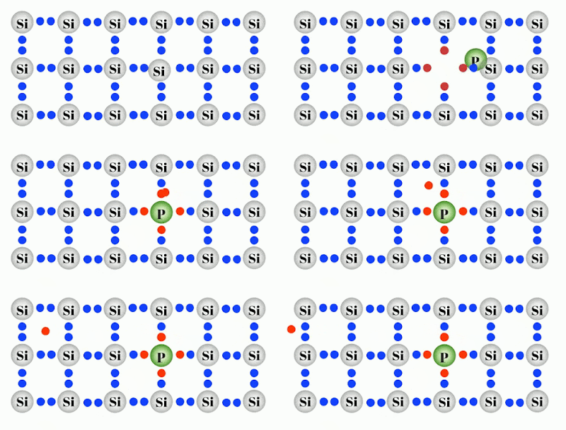
Intrinsic Semiconductors An intrinsic semiconductor is an undoped semiconductor. This means that holes in the valence band are vacancies created by electrons that have been thermally excited to the conduction band, as opposed to doped semiconductors where holes or electrons are supplied by a “foreign” atom acting as an impurity. The only way the Intrinsic semiconductors conduct electricity is by their own valance electron moving freely inside the lattice structure as shown in above gif.
So now you would ask- What is Doping? well... Let me Explain
Doping is basically adding different atoms to the intrinsic or pure atoms like Silicon to the defined modification of conductivity. Two of the most important materials silicon can be doped with, are boron (3 valence electrons = 3-valent) and phosphorus (5 valence electrons = 5-valent). Other materials are aluminum, indium (3-valent) and arsenic, antimony (5-valent). The doped material is referred to as an extrinsic semiconductor.
So there happens to be two types of Extrinsic semiconductors:
1) Positively Doped semiconductors
2) Negatively Doped semiconductors
Positively Doped semiconductors are the ones which has been doped with atom having 3 valance electrons like Boron which creates a positively charged holes in the structure. The holes tend to conduct electricity as the elections try to fill the holes and generate new holes.
 |
| The direction of the current is the direction of flow of holes. (In this case current flows from of right to left) |
Negatively Doped semiconductor are the ones which has been doped by the atom having 5 valance electron such as Phosphorus which makes an electron free per Phosphorus atom as shown in figure. This electron conducts electric current freely and behaves as a conductor more than a semiconductor.
 |
| The direction of the current is opposite to the flow of electron. (In this case, current flows from left to right.) |
Now the lets explore the possibilities created using this P and N type doped semiconductors.
An unbiased Diode
A diode is a two-terminal component that conducts current primarily in one direction; it has
low resistance in one direction, and high resistance in the other. the structure of the diode is like this
It would be easy to understand if it was just that. But its not the case.
There is a P-N Junction between both types of doped materials.
To be continued soon in next update.... about the PN junction diode.
Thanks and see you again.
~~~~~~~~~~~~~~~~~~~~~~~~~~~~~~
Did you know: Walking across a carpet can generate up to 35,000 V of static electricity.


Comments
Post a Comment